To continue Moore’s law, transistor scaling needs to be enabled by geometry innovations. From the 22nm node, bulk FinFET, a multi-gate transistor built on a silicon substrate, has replaced planar FET and become mainstream for mobile SoC applications [1-3]. Beyond the 3nm nodes, bulk gate-all-around (GAA) technology has emerged as a promising transistor architecture, offering superior electrostatic and leakage control [4-8]. Vertically stacked horizontal nanosheets (NS) further enhance driving current per layout footprint [8-11]. CMOS technology scaling will no longer be limited at the transistor level to continue the roadmap further.
New scaling options in considerations of technology co-optimization (DTCO) and system-technology co-optimization (STCO) are being explored to achieve more tailored chip and enhanced system performance, such as a backside power delivery network (BS-PDN). This article examines the impact of double-sided connectivity with BS-PDN on ESD reliability.
Backside Power Delivery Network
BS-PDN was introduced as part of DTCO to enhance functional performance in logic scaling [12]. Metal routing is simplified by separating power and signal pathways, improving frontside (FS) signal integrity, and optimizing backside power delivery [13]. A high-density through silicon via (TSV) or power via is critical for double-sided connectivity between the silicon wafer’s front and back sides. Thinning the wafer to just a few hundred nanometers is necessary to maintain TSV process quality by achieving a proper aspect ratio [14].
Figure 1 illustrates the simplified process flow for achieving a thinned silicon thickness of 300nm and double-sided connectivity with nano-TSV (nTSV) structures. However, reducing the silicon substrate thickness could challenge ESD robustness, as ESD protection devices rely on sufficient Si substrate volume for effective discharge and heat dissipation. Unlike fully depleted silicon-on-insulator (FD-SOI) technology, which allows an open buried oxide layer (BOX) to enhance ESD performance, this option is not viable for double-sided connectivity with BS-PDN [14].
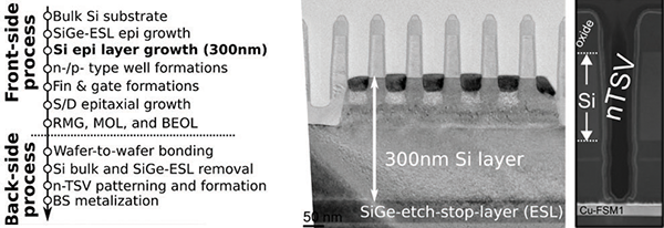 Figure 1
Impact of Extremely Thinned Silicon Substrates on ESD Diode Performance
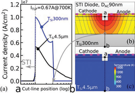
Recent studies have examined the ESD performance of two typical protection diodes—shallow trench isolation (STI) and gated diodes—with extremely thinned silicon substrates [15]. Figure 2(a) on page 48 shows the simulation results of STI diodes with 300nm and 4.5µm substrate thicknesses. The diodes are stressed by a 100-ns TLP stress. The injected TLP current is 0.67A, corresponding to a 1-kV HBM event. The 4.5µm represents the conventional full Si wafer thickness because it is longer than the thermal diffusion length (~3µm) of 100-ns TLP stress [16]. The current density in the thinned STI diode is approximately twice as high as that of the thick diode. In Figures 2(b) and 2(c), the simulation results show that the thinned STI diode certainly fails at 0.67A TLP current, while the thick STI diode remains at a much lower temperature.
For gated diodes, the simulation results (Figure 3) indicate that current penetration beyond 300nm is minimal, suggesting smaller performance degradation compared to STI diodes. Furthermore, the lattice temperature in the thinned gated diode is much lower than in the thinned STI diode.
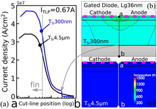 Figure 3
Proposed Solution: ESD Diodes with Active Backside Technology
In response to these ESD challenges from substrate thinning and BS-PDN, active backside (BS) technology has been proposed by introducing a p+ epitaxial layer and BS contact patterning (Figure 4) [17]. The vertical diode can thus be enabled offering significant advantages, such as improved area efficiency and ESD current uniformity. Moreover, the vertical diode’s design facilitates better thermal dissipation by incorporating backside metal layers (BSM) as heat sinks (Figure 5). This simulation decouples the impact of heat dissipation from the frontside metals (FSM).
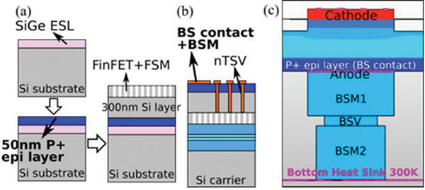 Figure 4
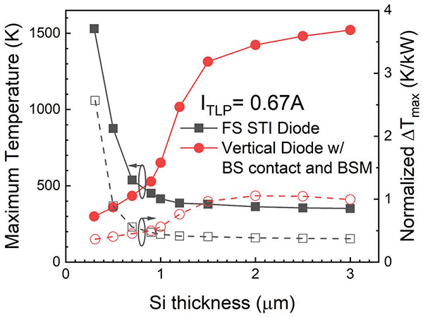 Figure 5
Simulations show that the maximum temperature (Tmax) and normalized increased temperature (∆Tmax) of the vertical diode decrease with reduced silicon thickness, demonstrating substrate thinning is beneficial to vertical ESD diode, especially in extremely thinned Si substrate.
Future ESD Challenges in DTCO and STCO Scaling
Looking ahead, GAA technology is expected to evolve further. A recent proposal includes a fork-shaped transistor architecture to minimize spacing between p-type and n-type MOSFETs, offering superior scalability compared to current nanosheet architectures [12, 18]. Additionally, complementary FET (CFET) technology, which stacks n-type MOSFETs on top of p-type MOSFETs, eliminates the n-to-p separation bottleneck, significantly reducing the standard cell area footprint (Figure 6).

However, CFET technology presents two key challenges for ESD robustness. First, the thin nanosheet structure and absence of a body terminal limit ESD discharge through parasitic devices, forcing current to discharge through the active channel. Second, the complete isolation between n-type and p-type active regions complicates ESD diode implementation, requiring special process options that may not be compatible with standard flows.
References
- S. Natarajan et al., “A 14nm logic technology featuring 2nd-generation FinFET, air-gapped interconnects, self-aligned double patterning and a 0.0588 µm2 SRAM cell size,” in IEDM Tech. Dig., 2014, p. 3.7.1-3.7.3.
- C. Auth et al., “A 22nm high performance and low-power CMOS technology featuring fully-depleted tri-gate transistors, self-aligned contacts and high density MIM capacitors,” in VLSI Tech. Dig., 2012, p. 131-132.
- E. Rosseel et al., “Characterization of Epitaxial Si:C:P and Si:P Layers for Source/Drain Formation in Advanced Bulk FinFETs,” ECS Transactions, vol. 64, no. 6, p. 977-987, 2014.
- K. J. Kuhn, “Considerations for Ultimate CMOS Scaling” IEEE Trans. on Electron Devices, vol. 59, no. 7, p. 1813, 2012.
- S.-G. Hur et al., “A practical Si nanowire technology with nanowire-on-insulator structure for beyond 10nm logic technologies,” in IEDM Tech. Dig., 2013, p. 646.
- I. Lauer et al., “Si nanowire CMOS fabricated with minimal deviation from RMG FinFET technology showing record performance,” in VLSI Tech. Dig., 2015, p. 142.
- H. Mertens et al., “Gate-all-around MOSFETs based on vertically stacked horizontal Si nanowires in a replacement metal gate process on bulk Si substrates,” in VLSI Tech. Dig., 2016, p. 142.
- C. Dupre et al., “15nm-diameter 3D stacked nanowires with independent gates operation: ΦFET”, in IEDM Tech. Dig., 2008, p. 749.
- H. Mertens et al., “Vertically stacked gate-all-around Si nanowire CMOS transistors with dual work function metal gates,” in IEDM Tech. Dig., 2016, p. 158
- N. Loubet et al., “Stacked nanosheet gate-all-around transistor to enable scaling beyond FinFET,” in VLSI Tech. Dig., 2017, p. T-230-231.
- R. Ritzenthaler et al., “Vertically Stacked Gate-All-Around Si Nanowire CMOS Transistors with Reduced Vertical Nanowires Separation, New Work Function Metal Gate Solutions, and DC/AC Performance Optimization,” in IEDM Tech. Dig. 2018, p. 508.
- J. Ryckaert et al., “Enabling Sub-5nm CMOS Technology Scaling Thinner and Taller!” in IEDM Tech. Dig., 2019, p. 685.
- A. Mallik et al., “The impact of sequential-3D integration on semiconductor scaling roadmap,” in IEDM Tech. Dig., 2017.
- A. Veloso et al., “Enabling Logic with Backside Connectivity via n-TSVs and its Potential as a Scaling Booster,” in VLSI Tech. Dig., 2021.
- W.-C. Chen et al., “ESD Challenges in 300nm Si Substrate of DTCO/STCO Scaling Options”, in IEDM Tech. Dig., 2023.
- G. Hellings et al., “Concise Analytical Expression for Wunsch-Bell 1-D Pulsed Heating and Applications in ESD Using TLP,” in Proc. of IRPS, 2019.
- K. Serbulova et al., “Enabling Active Backside Technology for ESD and LU Reliability in DTCO/STCO,” in VLSI Tech. Dig., 2022.
- P. Weckx et al., “Novel forksheet device architecture as ultimate logic scaling device towards 2nm,” in IEDM Tech. Dig., 2019, p. 871.
